How Can Printed Circuit Board Assembly Accomplish High-Density Interconnects?
Printed Circuit Board Assembly Accomplish High-Density Interconnects
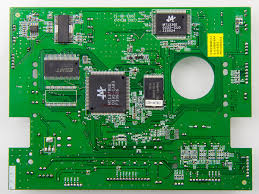
Assembled into electronic devices like computers, tablets, smartwatches and appliances, printed circuit boards (PCB) support electrical interfaces for a wide range of functions. They are also used for data and communication networks, aerospace systems and automobiles. The basic PCB design is an insulating base on which conducting metal tracks are patterned to form electrical connections for components mounted to the top or bottom of the base. Those connections are made with copper pads and solder. Printed circuit board assembly involves the application of solder paste, a thin layer of metal powder that is deposited onto each pad. The paste is then melted by the application of heat from the reflow oven, which fuses the solder to the pad. Once cooled, the solder mask is removed and the soldered areas are exposed.
The process of assembling a printed circuit board assembly requires careful considerations to minimize the possibility of errors and rework. This is especially important when dealing with high-density interconnects (HDI). HDI technology increases the number of signal traces on a board and offers benefits such as lower power supply noise, higher signaling frequencies and improved electromagnetic radiation decoupling. However, there are unique manufacturing constraints associated with HDI technology that must be considered in the PCB design and assembly process.
These constraints include the choice of materials and component placement, the use of buried or blind holes, and the distribution of micro vias. In addition, the routing of high-speed signals needs special attention to reduce impedance discontinuities and excess electromagnet emissions. It is important to plan for these issues during the PCB layout and design phase so that any problems can be corrected before fabrication begins.
How Can Printed Circuit Board Assembly Accomplish High-Density Interconnects?
Another key consideration is the type of soldering used for the traces. Although most PCBs are assembled using surface-mount components, some designs may contain through-hole components with long wire leads. If the through-hole components are sensitive to the wave soldering process, it is important to clearly note this in the PCB design.
Lastly, it is important to account for thermal effects. As a circuit board is energized, it will begin to generate heat that can affect the performance of the circuit. This can be avoided by proper component placement and by using thermal sinks to dissipate the heat. Printed Circuit Board Assembly (PCBA) is a crucial process in electronics manufacturing, where individual electronic components are soldered onto a bare PCB to create functional electronic devices. This intricate process is at the heart of modern electronics, enabling the creation of everything from smartphones and laptops to medical devices and automotive systems.
If you have questions about your printed circuit board design, contact a professional PCB engineer for help. At Altest, we offer a free DFM check to review your design and make sure it is ready for fabrication. Our engineers will check for part spacing, pin indications, footprint corroboration and bill of materials verification among other things. This can help you avoid costly mistakes and delays in the fab and assembly process. Contact us today to get started!