What Are the Limitations of HDI PCB Technology?
Limitations of HDI PCB Technology
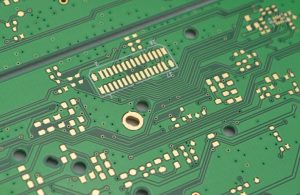
High-density interconnect (HDI) PCB technology allows electronic manufacturers to reduce board size, while delivering increased performance and reliability. This is accomplished through smaller component sizes, fine pitch packages and the use of blind and buried vias. This allows designers to pack more components in a small space, thus lowering the overall cost of production. In addition, HDI PCBs offer improved signal transmission through shorter trace lengths and decreased impedance paths.
However, the design and manufacturing process for hdi pcb circuit boards can be complex and challenging to learn. To ensure the best results, it is important to have an experienced manufacturer on your team. PCBONLINE can help you create a reliable HDI printed circuit board from start to finish.
The HDI fabrication process is similar to other types of PCBs, with the exception of sequential lamination and technologies for creating stacked vias and in-hole metallization. During the lamination process, each layer of core material is coated with dry resist. The dry resist is then applied to the surface of each layer using heated rolls, followed by a curing cycle. The PCB manufacturer then drills the resulting vias. This process requires much more precision than standard PCBs.
What Are the Limitations of HDI PCB Technology?
One of the most important considerations when designing an HDI circuit board is selecting the proper components. The choice of SMD components with low pin counts and BGA components with low pitches helps to reduce the size of the traces on the circuit board. It also helps to minimize the number of microvias and buried vias on the board, as this can reduce the amount of space required for routing.
Another key factor to consider when designing an HDI circuit board is ensuring that the conductive path can handle the expected signal levels and frequency. This is done by limiting the trace widths to what is necessary and making sure that there are enough ground planes for power, digital and analog signals. It is also important to keep in mind that the underlying dielectric layers must be able to withstand accelerated thermal cycles, multiple reflows and solder floats.
Finally, it is essential to choose the appropriate manufacturing techniques when designing an HDI circuit board. The choice of vias, through-holes and microvias, as well as the stackup height and number of layers, will significantly impact the manufacturing costs. In addition, the type of material used for the insulating layer must be compatible with the core substrate material to avoid issues with corrosion.
Lastly, HDI circuit boards can require more manual routing than traditional PCBs due to the smaller dimensions and fine pitch of the components. To ensure that the circuit board can be manufactured in a timely manner, it is important to work with an experienced, reliable manufacturer who can provide detailed information on the complexities of the manufacturing process. This will help to speed up the production time and reduce the amount of time required for testing, debugging, and repairs.